> For the complete documentation index, see [llms.txt](https://docs.ifreeq.com/llms.txt). Markdown versions of documentation pages are available by appending `.md` to page URLs; this page is available as [Markdown](https://docs.ifreeq.com/developer/device-development/access-mode-mcu/wi-fi-general-solution/hardware-design-reference-wi-fi.md).
# Hardware Design Reference Wi-Fi
## TYWE1S Module & MCU serial communication instructions
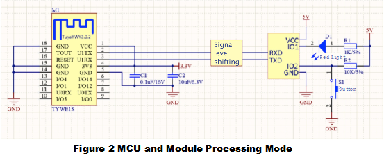
### 1.Typical Application diagram
Diagram 1 Module self-processing mode
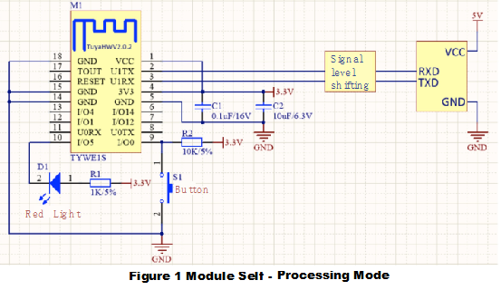
Diagram 2 MCU & Module cooperative processing mode
### 2.Design specification
1. Module power supply consumption: 3.3V/100mA, instantaneous current(5us) 450mA. Proposed supply current≥300mA.
2. Power filter capacitor C1 & C2 should be distributed as close to the 3V3 pin as possible.
3. Serial port U1TX & U1RX are user interface. Default setting Baud rate: 9600, Data level: 8 bit, Stop bit: 1 bit, No check bit, No flow control. **If you need to use serial port 1 as a common IO port, please contact with the business.**
4. Serial port U0TX & U0RX are the interface related module printing, please don't link to user serial port
**U0TX pin can't be used as an ordinary IO port, please suspend.** **if need to use U0RX pin as an ordinary IO port, please contact with the business.**
5. TOUT pin is voltage collection pin, can't be used as an ordinary IO port. **If idle, plesase suspend.**
6. IO 0 participates in the module for normal startup, when the power is on, this pin's level needs the high level for normal startup. For the export, a pull-up resistor is recommended. For the import, the input level should be considered. If idle, it can be suspended processing.
7. RESET pin is module hardware reset pin, effective under the low level. Without external circuitry, it can be directly connected to the IO port of MCU for use.
8. The module also needs the button and Wi-Fi status indicator. The button is used to clear network information of the module. The indicator is used to indicate the current status of the Wi-Fi module. If choose the module self-processing mode, refer to Diagram 1. If choose MCU & Module cooperative processing mode, refer to Diagram 2. Mode instructions can refer to "3.3 Query module work mode of MCU settings" in "Tuya general serial communication protocol".
9. If MCU supply voltage is 3.3V, circuit section about the signal level conversion in the reference diagram can be omitted.
10. Other idle pins can be suspended processing.
11. For Diagram 3, the antenna is susceptible to the shadow part of the package, don't wire and cover with copper, so as not to affect the antenna performance.
12. The exposed measuring point is located on the back of the module, as shown in Diagram 3 - The purple ring of TYWE1S recommended packaging. Please pay attention to avoidance when wiring. **Note: if need to recommend package, download it online or achieve it from the business.**
### 3.Antenna area instructions
Diagram 3 The shadow part is susceptible area for antenna, please don't wire and cover with copper. If the structure allows, please empty this area of PCB, so as not to affect the antenna performance.

## TYWE3S Module & MCU serial communication instructions
### Typical Application diagram
Diagram 1 Module self-processing mode
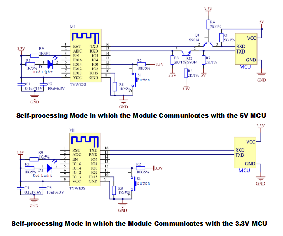
Diagram 2 MCU & Module cooperative processing mode

### Design specification
1. Module power supply consumption:3.3V/100mA, instantaneous current(5us) 450mA. Proposed supply current≥300mA.
2. Power filter capacitor C1 & C2 should be distributed as close to VCC pin as possible.
3. Serial port TXD & RXD are communication ports. At startup, there will be a lot of module information data output. Default setting Baud rate: 9600, Data level: 8 bit, Stop bit: 1 bit, No check bit, No flow control.
4. ADC pin is voltage collection pin, can't be used as normal IO function. If idle, it needs to be suspended.
5. IO 0 participates in the module for normal startup, when the power is on, this pin's level needs the high level for normal startup. For the export, a pull-up resistor is recommended. For the import, the input level should be considered. If idle, it can be suspended processing.
6. IO 2 participates in the module for normal startup, when the power is on, this pin's level needs the high level for normal startup. The default mode is module debugging port, and data output is available on the upper current. If idle, it can be suspended processing.
7. IO 15 participates in the module for normal startup, When the power is on, the pin's level needs the low level for normal startup. You need to add a pull-down resistor to your pin.
8. RST pin is module hardware reset pin, reset under the low level. For use, it can be directly connected to MCU's IO port without external circuit.
9. **Please note that there is no pull-up resistor inside of IO16 when used**
10. The module also needs the button and Wi-Fi status indicator. The button is used to clear network information of the module. The indicator is used to indicate the current status of the Wi-Fi module. If choose the module self-processing mode, refer to Diagram 1. If choose MCU & Module cooperative processing mode, refer to Diagram 2. Mode instructions can refer to "3.3 Query module work mode of MCU settings" in "Tuya general serial communication protocol".
11. If MCU supply voltage is 3.3V, circuit section about the signal level conversion in the reference diagram can be omitted.
12. The pins 9-14 need to be suspended, and other idle pins also need to be suspended.
13. Figure 3 the ANTENNA part is the position of antenna, which is forbidden to cover the copper & wire. It's better to empty this area of PCB, so as not to affect the antenna performance.
### Packaging instructions
Diagram 3 TYWE3S boundary dimension

**Note:if need recommended packaging, download from Internet or contact with the business.**
## Serial Port Communication Between the TYLC4 Module and MCU
### Typical Application Diagram
Figure 1-1 and Figure 1-2 show communication between the TYLC4 module and MCU in Wi-Fi module processing mode. Figure 1-3 and Figure 1-4 show communication between the module and MCU in cooperative processing mode.
S1 indicates the Wi-Fi module reset button, and LED1 indicates the Wi-Fi module status indicator. The following table lists the default mAppings between the LED1 status and working status of the Wi-Fi module.
| **LED1 Status** | **LED1 Display** | **Wi-Fi Module Status** |
| --------------- | --------------------------------------- | -------------------------- |
| Blinks quickly | Flashes on and off at 250 ms intervals | SmartConfig mode |
| Blinks slowly | Flashes on and off at 1500 ms intervals | AP mode |
| Steady on | Steady on | Connected to a router |
| Steady off | Steady off | Disconnected from a router |
Figure 1-1 Communication between the TYLC4 module and a 5 V MCU in Wi-Fi module processing mode
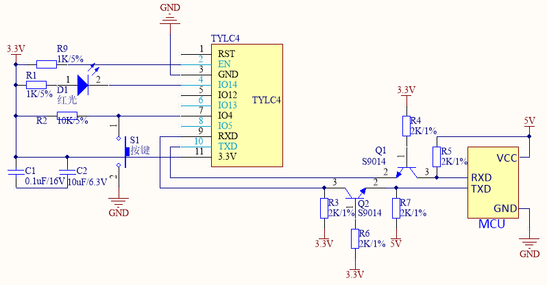
Figure 1-2 Communication between the TYLC4 module and a 3.3 V MCU in Wi-Fi module processing mode
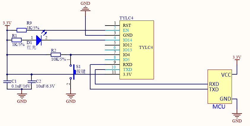
Figure 1-3 Communication between the TYLC4 module and a 5 V MCU in cooperative processing mode
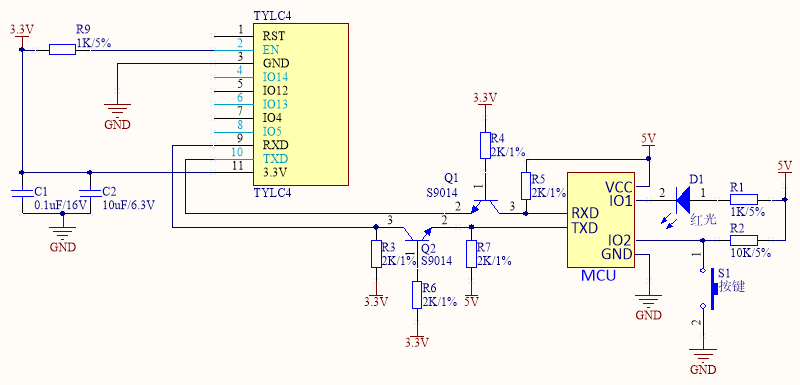
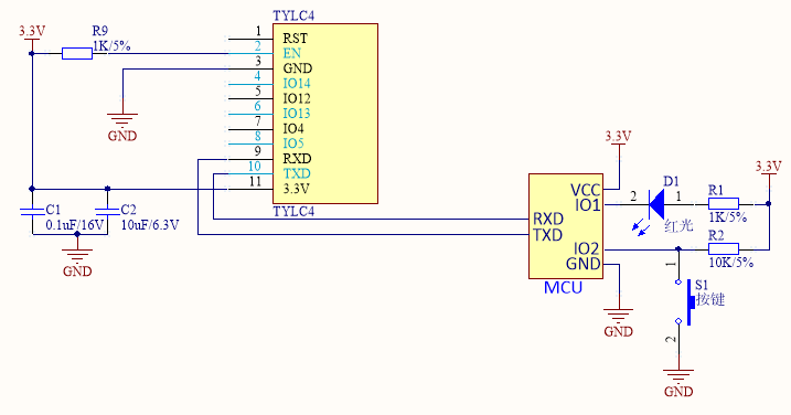
Figure 1-4 Communication between the TYLC4 module and a 3.3 V MCU in cooperative processing mode
### Design Description
1. The voltage and current for the Wi-Fi module to work properly are 3.3 V and 100 mA, respectively. It is recommended that the current be 300 mA or higher and that the total capacitance of external filter capacitors be more than 10 μF when the voltage is 3.3 V. When the Wi-Fi module is transmitting or receiving RF signals at 3.3 V, the current is increased by over 50%.
2. When designing the PCB layout, ensure that the filter capacitors C1 and C2 are as close to the VCC pin as possible.
3. The default settings for connections between the serial ports (TXD and RXD) and MCU are as follows:
Baud rate: 9600
Data bit: 8
Stop bit: 1
Parity bit: none
Flow control: none
For details, see *Tuya General Serial Port Communication Protocols*. When the Wi-Fi module is powered on, the TXD pin prints the module startup information. Skip the information during module startup. To use the serial port as a common I/O port, contact Tuya R\&D personnel.
4. The RST pin resets the module at low level. To use the RST pin, connect it to the I/O port of the MCU and low level input.
5. To use the module, you need a button and Wi-Fi status indicator.
The button (S1 in Figure 1-1 and Figure 1-2) is used to clear the module's network configuration. You can use the smart product's network connection button.
The indicator (LED1 in Figure 1-1 and Figure 1-2) indicates the working status of the Wi-Fi module or smart product.
For details about the processing modes, see section 3.3 in *Tuya General Serial Port Communication Protocols*.
6. If the input voltage of the MCU is 3.3 V, skip signal level conversion in Figure 1-1 and Figure 1-3.
7. Other idle pins can be vacant.
## TYWE2S Module & MCU serial communication instructions
### Typical Application diagram
Diagram 1 MCU(3.3V) & Module cooperative processing mode

Diagram 2 MCU(5V) & Module cooperative processing mode

### Design specification
1. Module power supply consumption: 3.3V, instantaneous current (5us) 451mA. Proposed supply current≥600mA.
2. Power filter capacitor C1 & C2 should be distributed as close to the 3.3V pin as possible.C1 & C2≥10uF.
3. RESET pin is module hardware reset pin, effective under the low level. Without external circuitry, it can be directly connected to the IO port of MCU for use.
## TYJW1 Module & MCU serial communication instructions
### Typical Application diagram
Diagram 1 MCU(3.3V) & Module cooperative processing mode
!\[image.png]
Diagram 2 MCU(5V) & Module cooperative processing mode

### Design specification
1. Module power supply consumption: 5V, instantaneous current(5us) 451mA. Proposed supply current≥600mA.
2. Power filter capacitor C1 & C2 should be distributed as close to the 5V pin as possible.C1 & C2≥10uF.
3. RESET pin is module hardware reset pin, effective under the low level. Without external circuitry, it can be directly connected to the IO port of MCU for use.
## TYJW2.0 Module & MCU serial communication instructions
### Typical Application diagram
Diagram 1 MCU(3.3V) & Module cooperative processing mode

Diagram 2 MCU(5V) & Module cooperative processing mode

### Design specification
1. Module power supply consumption: 5V, instantaneous current(5us) 451mA. Proposed supply current≥600mA.
2. Power filter capacitor C1 & C2 should be distributed as close to the 5V pin as possible.C1 & C2≥10uF.
3. RESET pin is module hardware reset pin, effective under the low level. Without external circuitry, it can be directly connected to the IO port of MCU for use.
## TYJW2.1 Module & MCU serial communication instructions
### Typical Application diagram
Diagram 1 MCU(3.3V) & Module cooperative processing mode

Diagram 2 MCU(5V) & Module cooperative processing mode

### Design specification
1. Module power supply consumption: 5V, instantaneous current(5us) 451mA. Proposed supply current≥600mA.
2. Power filter capacitor C1 & C2 should be distributed as close to the 5V pin as possible.C1 & C2≥10uF.
3. RESET pin is module hardware reset pin, effective under the low level. Without external circuitry, it can be directly connected to the IO port of MCU for use.
## TYJW2S-3.3V Module & MCU serial communication instructions
### Typical Application diagram
Diagram 1 MCU(3.3V) & Module cooperative processing mode

Diagram 2 MCU(5V) & Module cooperative processing mode

### Design specification
1. Module power supply consumption: 3.3V, instantaneous current(5us) 451mA. Proposed supply current≥600mA.
2. Power filter capacitor C1 & C2 should be distributed as close to the 3.3V pin as possible.C1 & C2≥10uF.
3. RESET pin is module hardware reset pin, effective under the low level. Without external circuitry, it can be directly connected to the IO port of MCU for use.
## TYJW2S-5V Module & MCU serial communication instructions
### Typical Application diagram
Diagram 1 MCU(3.3V) & Module cooperative processing mode

Diagram 2 MCU(5V) & Module cooperative processing mode

### Design specification
1. Module power supply consumption: 5V, instantaneous current(5us) 451mA. Proposed supply current≥600mA.
2. Power filter capacitor C1 & C2 should be distributed as close to the 5V pin as possible.C1 & C2≥10uF.
3. RESET pin is module hardware reset pin, effective under the low level. Without external circuitry, it can be directly connected to the IO port of MCU for use.
## WR1 Module & MCU serial communication instructions
### Typical Application diagram
Diagram 1 MCU(3.3V) & Module cooperative processing mode

Diagram 2 MCU(5V) & Module cooperative processing mode

### Design specification
1. Module power supply consumption: 3.3V,the maximum constant current295mA. Proposed supply current≥400mA.
2. Power filter capacitor C1 & C2 should be distributed as close to the 3.3V pin as possible.C1 & C2≥10uF.
## WR1E Module & MCU serial communication instructions
### Typical Application diagram
Diagram 1 MCU(3.3V) & Module cooperative processing mode

Diagram 2 MCU(5V) & Module cooperative processing mode

### Design specification
1. Module power supply consumption: 3.3V,the maximum constant current295mA. Proposed supply current≥400mA.
2. Power filter capacitor C1 & C2 should be distributed as close to the 3.3V pin as possible.C1 & C2≥10uF.
## WR2 Module & MCU serial communication instructions
### Typical Application diagram
Diagram 1 MCU(3.3V) & Module cooperative processing mode

Diagram 2 MCU(5V) & Module cooperative processing mode

### Design specification
1. Module power supply consumption: 3.3V,the maximum constant current295mA. Proposed supply current≥400mA.
2. Power filter capacitor C1 & C2 should be distributed as close to the 3.3V pin as possible.C1 & C2≥10uF.
## WR2E Module & MCU serial communication instructions
### Typical Application diagram
Diagram 1 MCU(3.3V) & Module cooperative processing mode

Diagram 2 MCU(5V) & Module cooperative processing mode

### Design specification
1. Module power supply consumption: 3.3V,the maximum constant current295mA. Proposed supply current≥400mA.
2. Power filter capacitor C1 & C2 should be distributed as close to the 3.3V pin as possible.C1 & C2≥10uF.
## WR3 Module & MCU serial communication instructions
### Typical Application diagram
Diagram 1 MCU(3.3V) & Module cooperative processing mode

Diagram 2 MCU(5V) & Module cooperative processing mode

### Design specification
1. Module power supply consumption: 3.3V,the maximum constant current295mA. Proposed supply current≥400mA.
2. Power filter capacitor C1 & C2 should be distributed as close to the 3.3V pin as possible.C1 & C2≥10uF.
## WR3E Module & MCU serial communication instructions
### Typical Application diagram
Diagram 1 MCU(3.3V) & Module cooperative processing mode
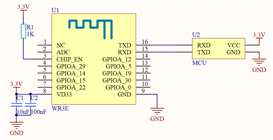
Diagram 2 MCU(5V) & Module cooperative processing mode

### Design specification
1. Module power supply consumption: 3.3V,the maximum constant current295mA. Proposed supply current≥400mA.
2. Power filter capacitor C1 & C2 should be distributed as close to the 3.3V pin as possible.C1 & C2≥10uF.
## WR4 Module & MCU serial communication instructions
### Typical Application diagram
Diagram 1 MCU(3.3V) & Module cooperative processing mode

Diagram 2 MCU(5V) & Module cooperative processing mode

### Design specification
1. Module power supply consumption: 3.3V,the maximum constant current295mA. Proposed supply current≥400mA.
2. Power filter capacitor C1 & C2 should be distributed as close to the 3.3V pin as possible.C1 & C2≥10uF.
## WRG1 Module & MCU serial communication instructions
### Typical Application diagram
Diagram 1 MCU(3.3V) & Module cooperative processing mode

Diagram 2 MCU(5V) & Module cooperative processing mode

### Design specification
1. Module power supply consumption: 3.3V,the maximum constant current295mA. Proposed supply current≥400mA.
2. Power filter capacitor C1 & C2 should be distributed as close to the 3.3V pin as possible.C1 & C2≥10uF.
## WBR1 Module & MCU serial communication instructions
### Typical Application diagram
Diagram 1 MCU(3.3V) & Module cooperative processing mode

Diagram 2 MCU(5V) & Module cooperative processing mode

### Design specification
1. Module power supply consumption: 3.3V,the maximum instant current is 324mA. Proposed supply current≥500mA.
2. Power filter capacitor C1 & C2 should be distributed as close to the 3.3V pin as possible.C1 & C2≥10uF.
## WBR1D Module & MCU serial communication instructions
### Typical Application diagram
Diagram 1 MCU(3.3V) & Module cooperative processing mode

Diagram 2 MCU(5V) & Module cooperative processing mode

### Design specification
1. Module power supply consumption: 3.3V,the maximum instant current is 392mA. Proposed supply current≥500mA.
2. Power filter capacitor C1 & C2 should be distributed as close to the 3.3V pin as possible.C1 & C2≥10uF.
## WBR2 Module & MCU serial communication instructions
### Typical Application diagram
Diagram 1 MCU(3.3V) & Module cooperative processing mode

Diagram 2 MCU(5V) & Module cooperative processing mode

### Design specificationi
1. Module power supply consumption: 3.3V,the maximum instant current is 324mA. Proposed supply current≥500mA.
2. Power filter capacitor C1 & C2 should be distributed as close to the 3.3V pin as possible.C1 & C2≥10uF.
## WBR2D Module & MCU serial communication instructions
### Typical Application diagram
Diagram 1 MCU(3.3V) & Module cooperative processing mode

Diagram 2 MCU(5V) & Module cooperative processing mode

### Design specification
1. Module power supply consumption: 3.3V,the maximum instant current is 392mA. Proposed supply current≥500mA.
2. Power filter capacitor C1 & C2 should be distributed as close to the 3.3V pin as possible.C1 & C2≥10uF.
## WBR3 Module & MCU serial communication instructions
### Typical Application diagram
Diagram 1 MCU(3.3V) & Module cooperative processing mode

Diagram 2 MCU(5V) & Module cooperative processing mode
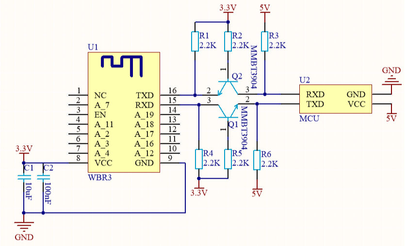
### Design specification
1. Module power supply consumption: 3.3V,the maximum instant current is 324mA. Proposed supply current≥500mA.
2. Power filter capacitor C1 & C2 should be distributed as close to the 3.3V pin as possible.C1 & C2≥10uF.
## WBR3D Module & MCU serial communication instructions
### Typical Application diagram
Diagram 1 MCU(3.3V) & Module cooperative processing mode

Diagram 2 MCU(5V) & Module cooperative processing mode

### Design specification
1. Module power supply consumption: 3.3V,the maximum instant current is 392mA. Proposed supply current≥500mA.
2. Power filter capacitor C1 & C2 should be distributed as close to the 3.3V pin as possible.C1 & C2≥10uF.