> For the complete documentation index, see [llms.txt](https://docs.ifreeq.com/llms.txt). Markdown versions of documentation pages are available by appending `.md` to page URLs; this page is available as [Markdown](https://docs.ifreeq.com/developer/smart-product-solution/voice-product/design-reference-materials-domestic-voice-module.md).
# Design Reference Materials - Domestic Voice Module
## Audio module VWXR2 hardware design guide
### Size package
VWXR2 consists of three rows of pins with the spacing of 1.5mm;
Size of M1:20mm (W) \*30mm (L) \*3.6mm (H).
The size drawing is shown in figure 1:

### Pin definition
The schematic diagram of the VWXR2 module is shown in the following figure

VWXR2 module pin definition
| Pin number | function | describe |
| ------------------- | ------------------------------------------------------------------- | ------------------------------------------------------------------------------------ |
| 1 | GPIO | GPIOA0 |
| 2 | GPIOA1 | |
| 3 | GPIOA2 | |
| 4 | GPIOA3 | |
| 5 | GPIOB16 | |
| 6 | GPIOB17(Default for the distribution of network & MAC - off button) | |
| 11 | RST | System reset, low level reset |
| 12 | PWM0 | PWM |
| 13 | PWM1 | PWM |
| 14 | PWM3 | PWM |
| 15 | PWM5 | PWM |
| 16 | PWM6 | PWM |
| 18 | SPK+ | |
| 19 | SPK- | |
| 21 | MIC1- | |
| 22 | MIC1+ | |
| 23 | MIC2+ | |
| 24 | MIC2- | |
| 27 | ADC\_CH5 | External analog signal detection |
| 28 | ADC\_CH0 | ADC Button interface |
| 30 | TWI0-SCL | I2C |
| 31 | TWI0-SDA | |
| 32 | IR\_RX | |
| 33 | IR\_TX | |
| 34 | UART0-TX | Log serial port, burning serial port |
| 35 | UART0-RX | |
| 36 | UART1\_RTS | Serial port 1, for MCU docking communication, the whole serial port for flow control |
| 37 | UART1\_CTS | |
| 38 | UART1\_RX | |
| 39 | UART1\_TX | |
| 7、10、17、20、25、26、29 | GND | GND |
| 8、9 | 5V | 5 v power supply |
**Instructions for the use of GPIO pins**
**1) GPIOB17 (default is the distribution of the network & MAC).**
**2) the network indicator light and the voice-related indicator light default PWM0 and PWM1, other applications can consider using PWM3/PWM5/PWM6 to do LED display light effect expansion (PWM will be better support for breathing light, if no breathing effect, GPIOA0/1/2/3/16 can also be used).**
**3) ADC\_CH5 can be used to collect external analog signals according to user requirements, and the input voltage is required to be less than 2.5v.**
**4) for applications with limited resources of GPIO, ADC\_CH0 can be used to connect multiple buttons with partial voltage according to the actual needs of customers to reduce the occupation of GPIO. Since the input withstand voltage is 2.5v, it is suggested to design the power rail of partial voltage connection method as 1.8v, that is, the external supply of 1.8v power is provided to design the button circuit of partial voltage.**
**5) PWM0/1/3/5/6 this 5-channel PWM can be used separately to drive RGBCW in lighting applications, i.e**
**PWM0 -- - > R red light**
**PWM1 -- - > G green light**
**PWM3 -- - > B blue light**
**PWM5 -- -- -- -- > C cool colors**
**PWM6 -- - > W warm color**
**6) the GPIO level of VWXR2 is 3.3v.**
### Reference design circuit
Minimum system design for the VWXR2 module

### Power supply design
Refer to vwxr2\_design\_reference.pdf above.

Here are some design considerations:
1\) the filter capacitor C7 should not be too small, and it is recommended to be over 10uF. Note that the withstand voltage should be 10V or above.
2\) considering that the source of power input to the module is unknown, if the power supply noise is relatively large, a magnetic bead can be considered.
3\) the ripple of vcc-5v voltage should not be too large, and should not exceed 5.5v, which may cause damage to the module. Please refer to the specification of the module for details.
4\) the VWXR2 module requires the power supply to output more than 5V/1A to ensure the stable operation of the equipment.
\*\* \*\*
### MIC selection recommendation and MIC circuit
The MIC circuit is shown below. This scheme recommends the elector MIC. The MIC selection can be referred to the following table. Of course, if users do not have high performance requirements, the selection parameters can be appropriately relaxed.
For the MIC circuit, in order to simplify the peripheral circuit, the peripheral circuit only needs to be designed as shown in the following figure, with ESD protection circuit and TDD inhibition circuit reserved.

### SPK circuit
The VWXR2 module integrates the class D power amplifier, which can generate 2W power with a 4-ohm horn under the condition of 5V power supply. The SPK design circuit is shown in the following figure.

Since the customer will have a variety of requirements on the horn, the selection is not too limited, but please note that the horn at rated power, THD should not be less than 10%.
### Microphone selection guide
#### Introduction of MIC selection parameters
The following is the specification of an electret MIC that our company has verified.

The parameters are:
1\) the higher the sensitivity is, the farther the pickup distance is, and the general requirement is no less than -30db. For those with low range requirements, electret MIC with slightly lower sensitivity can be selected: for example, -38db.
2\) S/N Ratio and signal-to-noise Ratio are generally not less than 64db. Low signal-to-noise ratio will affect the far-field pickup effect. If the pickup distance is not high, MIC with a lower SNR can be selected as the case may be.
#### Horn selection guide
It is difficult to recommend a standard scheme for horn selection, for the following reasons:
\1. Customers have different requirements on the size of the trumpet, which is usually limited by the ID.
\2. Customers have different requirements on the horn frequency ringing.
\3. Customers have different requirements for horn distortion.
, etc.
Here are some simple selection guidelines for your reference
\1. It is suggested that the speaker power should be controlled within 3W as far as possible (the speaker chamber should be attenuated more than 20dB to the microphone).
\2. The f0 of the speaker should be as low as possible, and the THD should be less than 10% within the range of 200HZ\~8KHZ (this requirement is for the non-speaker scheme. If it is used on the speaker, please refer to the selection guide of relevant documents for THD indicator).
\3. The horn and structure match is very precise. Please refer to the structural design document for the acoustic constraint rules between the cavity design of the relevant horn and MIC.
\4. If you don't have much experience in structure and cavity design, you can refer to spk-box.
### Reset circuit and distribution circuit
VWXR2 reset circuit can refer to the following figure, RST recommended to pull up to VCC\_BAT (usually 5V), low level reset, it is recommended to reserve ESD, please refer to vwxr2\_design\_referring.pdf for details.

VWXR2 distribution network and MAC keys, you can refer to the following figure, GPIO recommended to pull up to VCC\_CC (usually 3.3v), low level is effective, it is recommended to reserve ESD.

### Esd and TDD protection design
The following figure shows the MIC circuit ESD and TDD. ESD devices can be selected according to the product definition. The design is not recommended in this paper.

Capacitors of TDD circuit, C5,C6 and C4 are recommended to be reserved. If there is no space, can be removed, generally used for mobile phone filter TDMA 217Hz interference.
TDD supplement:
Some professional explanations about the role of the three capacitors of MIC can be used for reference:
1\) when the mobile phone is in the transmitting state, the whole mobile phone is in the strong magnetic field emitted by the mobile phone. Therefore, in addition to the anti-electric interference of the mobile phone itself, anti-electric interference is also proposed for MIC.
2\) in terms of design, the method of ice-clean capacitance between s-d is adopted. According to different frequencies, different capacitors are connected to each other. Generally, 10P and 33P capacitors are used in mobile phones for GSM mobile phones and two frequency bands, namely 900MHZ and 1800MHZ
### Module placement/antenna location
In order to ensure the optimization of RF performance, it is recommended that the distance between the module antenna and other metal parts should be at least 15mm. Since M1 is used by SMT process, it is pasted to the main control board and applied together with other components. Then the placement position and way of PCB antenna will directly affect RF performance. Here are the places we recommend and the places we don't. It is recommended to use the placement position of scheme 1 and scheme 2. The antenna is hollowed out outside the plate frame or near the antenna. The performance and individual module RF test performance is basically the same. If the design is limited, the PCB antenna must be placed on the bottom plate, you can refer to the placement method of plan 3. The antenna is in the plate frame, but there is no copper coating and wiring near the antenna. However, there is some loss of rf performance, which is about 1-2dbm attenuation. It is not recommended to use the placement position of plan 4, the antenna is in the plate frame, and the antenna is coated with copper or wire. The rf signal will be significantly attenuated.

Scheme 1: the antenna is outside the frame
Scheme 2: the antenna is placed along the edge of the plate, and the bottom is hollowed out

Scheme 3: the antenna is placed along the edge of the plate, and the bottom is not clad with copper
Scheme 4: the antenna plate is placed in the frame, and the bottom is hollowed out
\##Packaging instructions
The overall dimensions of VWXR2 are shown in the following figure

Note: 1) the unit of value in \[] is mm, and the unit of value outside \[] is inch
## Speech module - reference for acoustic structure design of product design
### Structural design
#### MIC cavity design
The Mic cavity is a very important part in acoustic design. FIG. 1 is a block diagram of MIC structure in a common product.
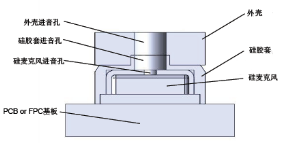FIG. 1 MIC structure in common products
The MIC pickup port to the surface of the product usually contains three parts: the acoustic seal part, the product enclosure part and the air passage part. The MESRF(Mic Enclosure System Resonant Frequency) has the greatest influence on microphone acoustic performance. The tolerance of components related to MIC within the product will directly affect MIC amplitude and frequency response.
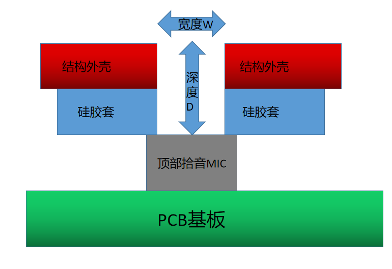FIG. 2 structure model diagram
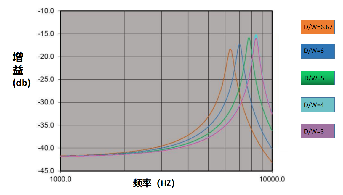
FIG. 3 influence curve of product MIC aperture to depth ratio on MESRF in FIG. 2
Several conclusions can be drawn from figure 2 and figure 3:
\1. The larger the opening of the product structure, the better, and the shorter the sound pickup channel, the better (for the consideration of ID aesthetics, there are usually some restrictions on the opening, and in the actual design, it is recommended to be more than 1.5mm).
\2. The design principle should try to ensure that it is within the range of human voice (the platform degree of frequency response within 8KHZ). The poor design of MIC pickup cavity leads to the front movement of MESRF resonance peak, which directly affects the back-end algorithm and ultimately affects the recognition effect.
Supplement: when designing the MIC chamber, it is usually necessary to add a dust screen. Dust screen selection, the number of options do not too much.
#### MIC sound insulation and shock absorption design
MIC damping and sound insulation design is divided into two aspects: damping and sound insulation.
**Damping**
\1. Generally, silica gel reference figure 2 is used for sound insulation and shock absorption. The hardness of silica gel shall be designed according to the compression amount of the actual structure.
\2. The MIC should be kept away from interference (exhaust fan) or vibration (horn vibration and structural vibration), so as to avoid major influence of structural vibration on the MIC.
**Sound insulation**
1、The microphone shall be isolated from the solid surface with silicone sleeve to reduce the vibration transmission and sealing of the shell. The design can refer to figure 4 to increase the contact between the silicone sleeve and the above structure.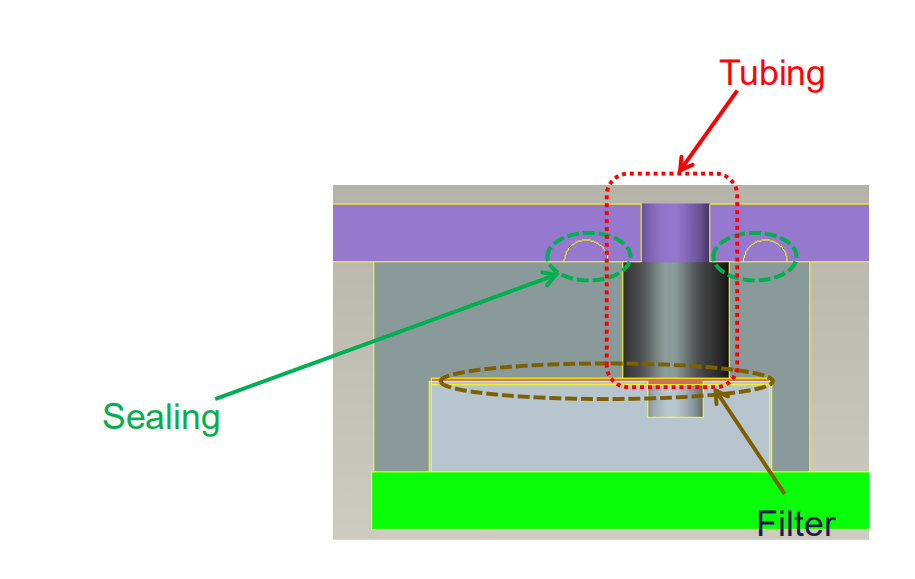
FIG. 4 increasing convex points of silicone sleeve
2, the silicone sleeve can increase the gum, prevent the silicone sleeve structure and shell in the assembly or use of relative movement, resulting in leakage.
\3. MIC must conduct internal sound insulation with SPK sound cavity to prevent the sound emitted by SPK from being directly transmitted to MIC through the internal space of the machine.
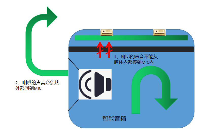
FIG. 5 view of sound insulation scheme
Note: for electret microphones, the protection of microphones should be considered in the structural design and production process to avoid the loss of microphone consistency caused by extrusion.
#### isolation design of MIC and SPK\*\*
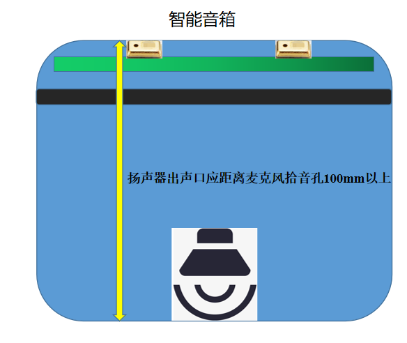
It is suggested that the loudspeaker and microphone should be placed in different cavities, and the cavities should be sealed with good sealing materials to prevent internal crosstalk. The loudspeaker mouthpiece should be more than 100mm away from the microphone sound pickup hole, the bigger the better. The speaker diaphragm and the passive diaphragm are not facing the microphone and the included Angle is greater than 90°.
#### SPK cavity design
Loudspeaker cavity design is also crucial, but due to the different requirements of sound quality, cavity structure and size vary, so this paper does not introduce in detail.
The requirement for sound quality and structure size is not high, so spk-box can be given priority to realize sound cavity design, which can greatly shorten the product development time.
In addition, the design of loudspeaker cavity should avoid the structural resonance caused by the sound, vibration. When the speaker cavity is loaded into the machine, be sure to carry out shock absorption treatment, such as the cable and screw for glue treatment.
When designing loudspeakers and passive radiators, the travel of the body should be fully considered, and the spacing of peripheral devices should be reserved to avoid abnormal sound and vibration under certain circumstances.